Tuesday, March 5, 2013

Static Mode Operation (Power Transistors)

Static Mode Operation

A power device is working in static mode when dc currents and voltages are applied to its terminals.


The above figure shows the schematic symbols, the terminal names, and the specific currents and voltages for BJT, MOSFET and IGBT.
Bipolar transistors are current controlled devices. In contrast, MOSFETs and IGBTs are voltage-driven devices. The performance characteristics of MOSFETs are generally superior to those of bipolar transistors: significantly faster switching times, higher input impedance, the absence of second breakdown, the ability to be paralleled, simpler drive circuitry.

Power BJT

Bipolar-based power devices include high-power bipolar transistors and Darlington transistors.

The current gain β of power bipolar transistors depends on the collector current IC. When the current increases, the current gain decreases as shown in the above figure.
To raise the current gain, Darlington transistors are used. Darlington transistors consist of two transistors connected in an emitter-follower configuration that share a common collector. The key advantage of the Darlington configuration is that the total current gain of the circuit equals the product of the current gain of both devices.

Power MOS Transistors as Switches

The behavior of enhancement-mode transistors depends on the applied gate-source voltage UGS. The n-MOS transistor is turned-off when UGS is smaller than the threshold voltage UT. There is no current and the device is replaced with an open switch. The inverse diode is inherent to the structure of power MOSFET and ensures a reverse-voltage blocking capability of the device.
When UGS > UT, the transistor is now turned-on. The key to MOSFET operation is the creation of the inversion channel beneath the gate; this allows current to flow. The region between the drain and source can be thought of as a resistor RON, although it does not behave in the same linear manner as a conventional resistor.

IGBT Characteristics

The above figure shows the equivalent circuit and static output I-V characteristics of an IGBT.
An IGBT is in a turn-off state if the gate-emitter voltage UGE is smaller than the threshold voltage UT. When UGE > UT the MOS transistor goes to turn-on. Then, the collector current from the IGBT flows through the series connected emitter-base junction of the PNP transistor, and subsequently through the drain-source channel of the MOS transistor. The output characteristics of IGBT devices are similar to those of MOSFET devices, but due to the series connected junction they are shifted approximately 0.7 V to the right. The output characteristics have two regions – the ohmic region (for small UCE values), and the saturation region (for high UCE values).

Safe Operating Area for BJT (Power Transistors)

Safe Operating Area (SOA) for BJT

The safe operating area (SOA) defines the current and voltage limitations of power devices.


The above figure shows the typical SOA of a power bipolar transistor. It can be partitioned into four regions. The maximum current limit (section a-b) and the maximum voltage limit (d-e) are determined by the technological features and construction of the particular device. The maximum power dissipation limits the product of the transistor's currents and voltages (section b-c). A secondary breakdown (c-d) occurs when high voltages and high currents appear simultaneously when the device is turned off. When this happens, a hot spot is formed and the device fails due to thermal runaway.

SOA for MOSFET & IGBT

The above figure shows the safe operating area (SOA) of MOSFET transistors. This area is bounded by three limits: current limit (section a-b), maximum power dissipation limit (b-c), and the voltage limits (c-d). The SOA of an IGBT is identical to that of the MOSFET SOA.
Since the drain current decreases when the temperature increases in MOSFET transistors, the possibility of secondary breakdown is almost nonexistent. If local heating occurs, the drain current - and consequently the power dissipation - both diminish. This avoids the creation of local hot spots that can cause thermal runaway.

The above figure demonstrates how the SOA of a device increases when the device is operating in pulse mode.
When the device is operating in DC mode the safe operating area is at its smallest. The SOA grows when pulse mode is used. The shorter the pulse signal, the higher the SOA.

Maximum Power Dissipation (Power Transistors)

Maximum Power Dissipation

High currents and voltages in power devices produce very high internal power loss. This loss occurs in the form of heat that must be dissipated; otherwise, the device can be destroyed as a result of overheating.


The maximum power dissipation Pmax indicates a device's maximum capability to transfer and conduct this power loss without overheating.
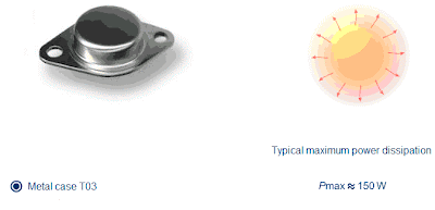
The above figure compares the power dissipation of different devices. As a device type is selected, the circular area changes to show the device's maximum power dissipation. As illustrated in the figure, larger metal cases are more efficient in removing heat from the transistor.

Thermal Resistance

Thermal resistance Rthj-a indicates the ability of the device to conduct and transfer heat from the junction (with temperature Tj) to ambient (with temperature Ta). More resistance means that less heat will dissipate.
The junction-to-ambient thermal resistance Rthj-a consists of two resistances: Rthj-c and Rthc-a in series. The Rthj-c is the junction-to-case thermal resistance. The Rthc-a is the case-to-ambient thermal resistance. The Rthc-a is many times higher than Rthj-c.
The above figure shows the values of Rthj-a for different packages. The particular value of each resistance depends on the type of materials and on the case size. Smaller values are typical for large metal cases.

Maximum Power Dissipation vs. Temperature


The maximum power dissipation Pmax of the transistor depends on the highest junction temperature that will not destroy the device Tjmax, the ambient temperature Ta, and the thermal resistance Rthj-a according to the equation shown in the above figure.
If the ambient temperature is less than or equal to 25°C the device reaches its maximum specified power rating. When the ambient temperature increases, the power rating decreases. If the ambient temperature Ta reaches the maximum junction temperature Tjmax, maximum power Pmax becomes zero.

Heat Sink

One way to increase the power rating of the device is to diminish the thermal resistance Rthj-a. A heat sink, which is usually a metal construction with a large surface area, is used to allow heat to dissipate to ambient more easily.
When a heat sink is present, the global thermal resistance Rthj-a decreases because there are more paths available for heat dissipation. The case-to-heat-sink thermal resistance Rthc-s and the heat-sink-to-ambient thermal resistance Rths-a both facilitate heat dissipation. As a result, the power rating increases as illustrated in the above figure.

Power Transistors

Power Transistors

Introduction


Power Transistors are electronics components that are use for the control and regulation of voltages and currents with high values. They are the basic components for the implementation of linear and switched mode power supplies, motor control circuits, automotive and aerospace systems, home appliances, and energy management systems

Why are Power Transistors Necessary?

Power Transistors are used to produce, convert, control and regulate high amounts of power output.Typical headphone amplifiers have a low output value (just a fraction of a watt). They are usually implemented with standard low power transistors.On the other hand, amplifiers with hundred-watt output power are used to ensure quality sound in large rooms or concert halls. These amplifiers operate with high-level currents and voltages (more than dozens of amperes and volts). The output stages of such amplifiers can be implemented only with power transistors.


Power Transistors are capable of providing high currents and high blocking voltages and therefore, high power. They can be classified into BJT (Bipolar Junction Transistors), MOSFET (Metal Oxide Semiconductor Field Effect Transistors), and devices such as IGBT (Insulated Gate Bipolar Transistors) that combine bipolar and MOS technologies.
The principle of operation behind high power transistors is conceptually the same as bipolar or MOS transistors. The main difference is that the active area of the power devices is distinctly higher, resulting in a much higher current handling capacity. For this reason, they have large packages.

Three Major Device Technologies

The above figure depicts the typical structure of BJT, MOSFET and IGBT devices.
For a BJT to maintain conduction, a high continuous current through the base region is required. This imposes the necessity of high power drive circuits.
MOSFETs and IGBTs are voltage-controlled devices. The IGBT has one more junction than the MOSFET, which allows for a higher blocking voltage but limits the switching frequency. In IGBTs, during conduction, the holes from the collector p+ region are injected into the n- region. The accumulated charge reduces IGBT's on-resistance and thus the collector-to-emitter voltage drop is also reduced.